ADC on the PIC32MZ post
So you want to use the ADC
If you've come from using the PIC32MX series, you'll remember that using the ADC was a simple affair. You could set it up in a few lines and then BAM it worked. And wow, the specs of the PIC32MX were merely:
- Fast and Accurate 16 channel 10-bit ADC
- Max 1 Mega sample per second at +/- 1LSB, conversion available during SLEEP & IDLE
But now with the MZ, take a look at this:
- 12-bit ADC Module
- 18 Msps rate with six Sample and Hold (S&H) circuits (five dedicated and one shared)
- Up to 48 analog inputs
- Multiple trigger sources
- Temperature sensor with ±2°C accuracy
Whooooooooooaaaaaa! 18 times the speed, 3 times the channels and even a temperature sensor. That is so cool! So you undoubtedly thought that, like the PIC32MX. the PIC32MZ would be simple too, maybe even use the same code. But, like everything else with the MZ, you're met with the cold, hard reality that
Microchip
hates
you
and doesn't want you to use one of their fastest PIC chips. You see, apart from the minor issue of the temperature sensor not working, at all, on any device, there's the matter of the insane way they've gone about implementing these 48 channels. To illustrate, here's what the map of the PIC32MX ADC hardware looks like:
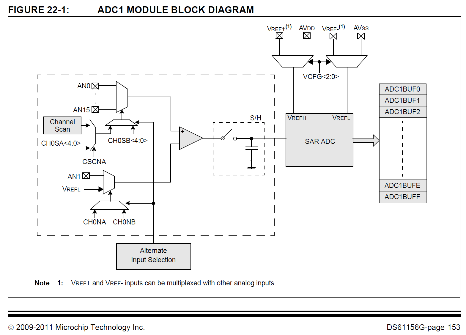
OK, so it's your typical Microchip block diagram. A bit confusing in places (and what's happening with AN1 there?) but it's not too bad. Now let's take a look at the new map for the PIC32MZ:
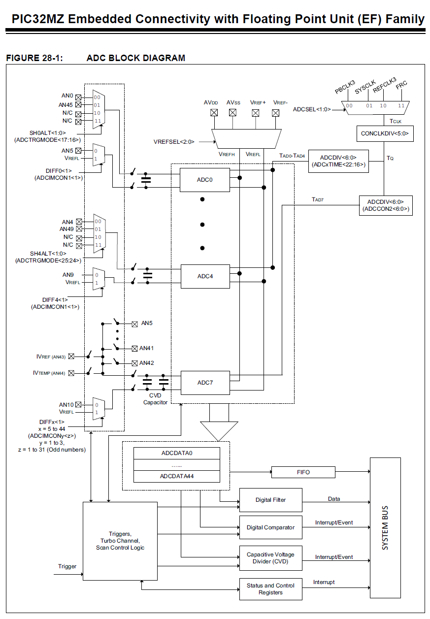
Ha. Ha. Ha. What a cruel joke. And this is the point where you run back to the safety of Harmony, only to realise multiple releases of Harmony also have bugs with the ADC code. Not even Microchip can get it working. But it's not just that it looks complicated, it actually is more complicated to use. But not impossible. In theory, this gives us more flexibility but the trade-off is that what used to take 3 lines to set up now takes a good deal more.
Secret Knowledge 1 - The ADC inputs are divided into classes
What you absolutely cannot tell from looking at that diagram is the on the PIC32MZ the ADC inputs are divided into the following classes:
- Class 1 - These inputs each have their own dedicated sample and holding hardware and can be triggered individually, are always sampling and will be converted as soon as you trigger them, independent of each other.
- Class 2 - These share ONE sample and hold unit, specificially ADC7, and can also be triggered individually but will only start sampling once you trigger them and even then, they have to take turns using ADC7 to do so.
- Class 3 - These also share ADC7
Furthermore, the inputs are divided as follows (for the PIC32MZ EF series):
- Class 1 = AN0 to AN4
- Class 2 = AN5 to AN31
- Class 3 = AN32 to AN44
Furthermore, the 18Msps speed is a bit fat bit of marketing speak as shown here:
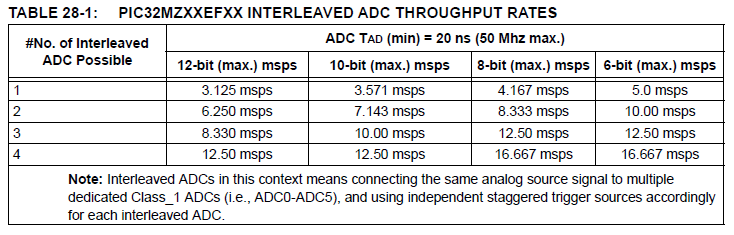
Even in their own datasheet they can't get 18msps, the closest they get is 16.67msps and that's only is you trigger 4 class 1 inputs at once, and even then only if they're in 6-bit mode. Ugh. Marketing sucks. But it's not all bad news!
How to use class 1 inputs on the PIC32MZ ADC
Today I'm going to just cover how to use class 1 inputs. Shockingly, the example in the ADC datasheet (DS60001344B) actually mostly works (apart from some key things that need to be set up first). Well, the class 1 one does. The class 2 one has typos in some of the register names. Because of course it does :)
In said example, AN0, AN1 and AN2 are set up and read into an array of integers called result[]. Let's take a look at said code from the datasheet:
int main(int argc, char** argv)
{
    int result[3];
    /* initialize ADC calibration setting */
    ADC0CFG = DEVADC0;
    ADC1CFG = DEVADC1;
    ADC2CFG = DEVADC2;
    ADC3CFG = DEVADC3;
    ADC4CFG = DEVADC4;
    ADC7CFG = DEVADC7;
    /* Configure ADCCON1 */
    ADCCON1 = 0; // No ADCCON1 features are enabled including: Stop-in-Idle, turbo,
    // CVD mode, Fractional mode and scan trigger source.
    /* Configure ADCCON2 */
    ADCCON2 = 0; // Since, we are using only the Class 1 inputs, no setting is
    // required for ADCDIV
    /* Initialize warm up time register */
    ADCANCON = 0;
    ADCANCONbits.WKUPCLKCNT = 5; // Wakeup exponent = 32 * TADx
    /* Clock setting */
    ADCCON3 = 0;
    ADCCON3bits.ADCSEL = 0; // Select input clock source
    ADCCON3bits.CONCLKDIV = 1; // Control clock frequency is half of input clock
    ADCCON3bits.VREFSEL = 0; // Select AVDD and AVSS as reference source
    /* Select ADC sample time and conversion clock */
    ADC0TIMEbits.ADCDIV = 1; // ADC0 clock frequency is half of control clock = TAD0
    ADC0TIMEbits.SAMC = 5; // ADC0 sampling time = 5 * TAD0
    ADC0TIMEbits.SELRES = 3; // ADC0 resolution is 12 bits
    ADC1TIMEbits.ADCDIV = 1; // ADC1 clock frequency is half of control clock = TAD1
    ADC1TIMEbits.SAMC = 5; // ADC1 sampling time = 5 * TAD1
    ADC1TIMEbits.SELRES = 3; // ADC1 resolution is 12 bits
    ADC2TIMEbits.ADCDIV = 1; // ADC2 clock frequency is half of control clock = TAD2
    ADC2TIMEbits.SAMC = 5; // ADC2 sampling time = 5 * TAD2
    ADC2TIMEbits.SELRES = 3; // ADC2 resolution is 12 bits
    /* Select analog input for ADC modules, no presync trigger, not sync sampling */
    ADCTRGMODEbits.SH0ALT = 0; // ADC0 = AN0
    ADCTRGMODEbits.SH1ALT = 0; // ADC1 = AN1
    ADCTRGMODEbits.SH2ALT = 0; // ADC2 = AN2
    /* Select ADC input mode */
    ADCIMCON1bits.SIGN0 = 0; // unsigned data format
    ADCIMCON1bits.DIFF0 = 0; // Single ended mode
    ADCIMCON1bits.SIGN1 = 0; // unsigned data format
    ADCIMCON1bits.DIFF1 = 0; // Single ended mode
    ADCIMCON1bits.SIGN2 = 0; // unsigned data format
    ADCIMCON1bits.DIFF2 = 0; // Single ended mode
    /* Configure ADCGIRQENx */
    ADCGIRQEN1 = 0; // No interrupts are used
    ADCGIRQEN2 = 0;
    /* Configure ADCCSSx */
    ADCCSS1 = 0; // No scanning is used
    ADCCSS2 = 0;
    /* Configure ADCCMPCONx */
    ADCCMPCON1 = 0; // No digital comparators are used. Setting the ADCCMPCONx
    ADCCMPCON2 = 0; // register to '0' ensures that the comparator is disabled.
    ADCCMPCON3 = 0; // Other registers are “don't care”.
    ADCCMPCON4 = 0;
    ADCCMPCON5 = 0;
    ADCCMPCON6 = 0;
    /* Configure ADCFLTRx */
    ADCFLTR1 = 0; // No oversampling filters are used.
    ADCFLTR2 = 0;
    ADCFLTR3 = 0;
    ADCFLTR4 = 0;
    ADCFLTR5 = 0;
    ADCFLTR6 = 0;
    /* Set up the trigger sources */
    ADCTRGSNSbits.LVL0 = 0; // Edge trigger
    ADCTRGSNSbits.LVL1 = 0; // Edge trigger
    ADCTRGSNSbits.LVL2 = 0; // Edge trigger
    ADCTRG1bits.TRGSRC0 = 1; // Set AN0 to trigger from software.
    ADCTRG1bits.TRGSRC1 = 1; // Set AN1 to trigger from software.
    ADCTRG1bits.TRGSRC2 = 1; // Set AN2 to trigger from software.
    /* Early interrupt */
    ADCEIEN1 = 0; // No early interrupt
    ADCEIEN2 = 0;
    /* Turn the ADC on */
    ADCCON1bits.ON = 1;
    /* Wait for voltage reference to be stable */
    while(!ADCCON2bits.BGVRRDY); // Wait until the reference voltage is ready
    while(ADCCON2bits.REFFLT); // Wait if there is a fault with the reference voltage
    /* Enable clock to analog circuit */
    ADCANCONbits.ANEN0 = 1; // Enable the clock to analog bias
    ADCANCONbits.ANEN1 = 1; // Enable the clock to analog bias
    ADCANCONbits.ANEN2 = 1; // Enable the clock to analog bias
    /* Wait for ADC to be ready */
    while(!ADCANCONbits.WKRDY0); // Wait until ADC0 is ready
    while(!ADCANCONbits.WKRDY1); // Wait until ADC1 is ready
    while(!ADCANCONbits.WKRDY2); // Wait until ADC2 is ready
    /* Enable the ADC module */
    ADCCON3bits.DIGEN0 = 1; // Enable ADC0
    ADCCON3bits.DIGEN1 = 1; // Enable ADC1
    ADCCON3bits.DIGEN2 = 1; // Enable ADC2
    while (1)
    {
        /* Trigger a conversion */
        ADCCON3bits.GSWTRG = 1;
        /* Wait the conversions to complete */
        while (ADCDSTAT1bits.ARDY0 == 0);
        /* fetch the result */
        result[0] = ADCDATA0;
        while (ADCDSTAT1bits.ARDY1 == 0);
        /* fetch the result */
        result[1] = ADCDATA1;
        while (ADCDSTAT1bits.ARDY2 == 0);
        /* fetch the result */
        result[2] = ADCDATA2;
        /*
        * Process results here
        *
        * Note: Loop time determines the sampling time since all inputs are Class 1.
        * If the loop time is small and the next trigger happens before the completion
        * of set sample time, the conversion will happen only after the sample time
        * has elapsed.
        *
        */
    }
    return (1);
}
OK...
...
70 lines of code to set up ADC0, ADC1 and ADC2. These are some big trade-offs but fine, fine, we'll take a look at it piece by piece. Important to note is that for some of this code the order of execution is very important so I recommend not changing it unless you know what you are doing. Also, on the EF devices there is no such thing as ADC5 and ADC6 so I've removed references to them from my code. With that, let's start:
/* initialize ADC calibration setting */
ADC0CFG = DEVADC0;
ADC1CFG = DEVADC1;
ADC2CFG = DEVADC2;
ADC3CFG = DEVADC3;
ADC4CFG = DEVADC4;
ADC7CFG = DEVADC7;
This sets up the 6 ADC units, ADC0 through ADC4 and ADC7, with their default values. Why you wouldn't do this automatically I don't know because on inspection of the datasheet ADCxCFG looks like this:
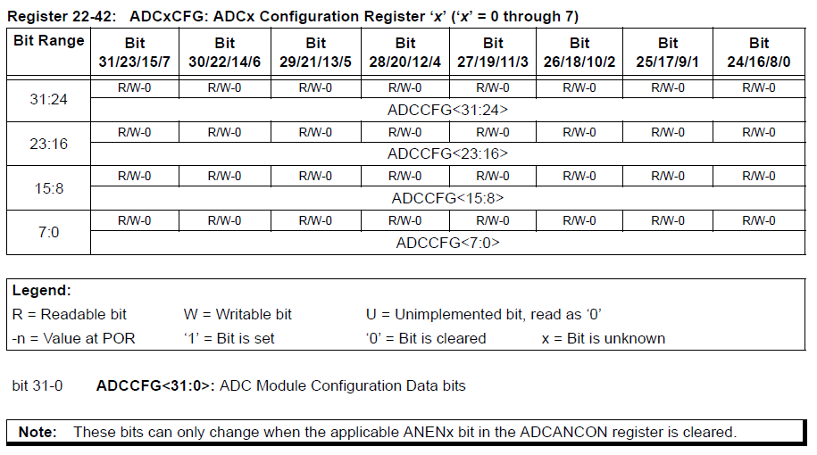
So while yes, you can change these there seems to be no reason to. Just classic Microchip design crashing into reality again.
/* Configure ADCCON1 */
ADCCON1 = 0; // No ADCCON1 features are enabled including: Stop-in-Idle, turbo,
// CVD mode, Fractional mode and scan trigger source.
/* Configure ADCCON2 */
ADCCON2 = 0; // Since, we are using only the Class 1 inputs, no setting is
// required for ADCDIV
Something very important to note in the set up of ADCCON1 and ADCCON2. We are only using class 1 inputs so no clock division stuff needs to be set upbut if you are using class 2 or 3 you will have to set up these as they control various aspects of ADC7.
/* Initialize warm up time register */
ADCANCON = 0;
ADCANCONbits.WKUPCLKCNT = 5; // Wakeup exponent = 32 * TADx
/* Clock setting */
ADCCON3 = 0;
ADCCON3bits.ADCSEL = 0; // Select input clock source
ADCCON3bits.CONCLKDIV = 1; // Control clock frequency is half of input clock
ADCCON3bits.VREFSEL = 0; // Select AVDD and AVSS as reference source
ADCANCON controls how long the ADC modules need to "warm up" before they can be used for conversion. Thankfully, this number is common to all ADCs on the PIC32MZ devices and is always set to 5 (which = 32TADx). As we will see later, it also contains the "enable" bits for ADCs 0 through 7 and status bits for whether they are ready or not.
For us and our class 1 example, ADCCON3 controls what to use as a voltage reference, what the clock frequency is and whether the digital outputs for each ADC module, again 0 through 7, are enabled or not.
/* Select ADC sample time and conversion clock */
ADC0TIMEbits.ADCDIV = 1; // ADC0 clock frequency is half of control clock = TAD0
ADC0TIMEbits.SAMC = 5; // ADC0 sampling time = 5 * TAD0
ADC0TIMEbits.SELRES = 3; // ADC0 resolution is 12 bits
ADC1TIMEbits.ADCDIV = 1; // ADC1 clock frequency is half of control clock = TAD1
ADC1TIMEbits.SAMC = 5; // ADC1 sampling time = 5 * TAD1
ADC1TIMEbits.SELRES = 3; // ADC1 resolution is 12 bits
ADC2TIMEbits.ADCDIV = 1; // ADC2 clock frequency is half of control clock = TAD2
ADC2TIMEbits.SAMC = 5; // ADC2 sampling time = 5 * TAD2
ADC2TIMEbits.SELRES = 3; // ADC2 resolution is 12 bits
As we're using AN0, AN1 and AN2, we need to set up timing information and resolution information for ADCs 0 through 2. Nothing complicated here.
/* Select analog input for ADC modules, no presync trigger, not sync sampling */
ADCTRGMODEbits.SH0ALT = 0; // ADC0 = AN0
ADCTRGMODEbits.SH1ALT = 0; // ADC1 = AN1
ADCTRGMODEbits.SH2ALT = 0; // ADC2 = AN2
Hmmm... what's this? There is some limited flexibility with ADCs 0 through 4. While, by default, AN0 is set up to be connected to ADC0, you can change SH0ALT to 1 to make ADC0 use pin AN45 instead. Similarly, you can:
- set SH1ALT to 0 / 1 to use AN1 / AN46,
- set SH2ALT to 0 / 1 to use AN2 / AN47,
- set SH3ALT to 0 / 1 to use AN3 / AN48 or
- set SH4ALT to 0 / 1 to use AN4 / AN49 respectively.
/* Select ADC input mode */
ADCIMCON1bits.SIGN0 = 0; // unsigned data format
ADCIMCON1bits.DIFF0 = 0; // Single ended mode
ADCIMCON1bits.SIGN1 = 0; // unsigned data format
ADCIMCON1bits.DIFF1 = 0; // Single ended mode
ADCIMCON1bits.SIGN2 = 0; // unsigned data format
ADCIMCON1bits.DIFF2 = 0; // Single ended mode
The FRACT and SIGN bits together make up the format in which the ADC will return data to you, according to this table:
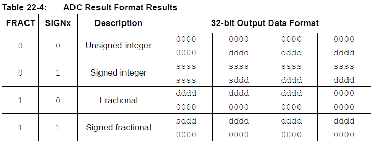
For our purpose, we just want a 12-bit integer, so we want them both set to 0 (FRACT is contained within ADCCON1 which we previously set to 0).
DIFF, as the name suggests, allows us to select between single-ended or differential inputs, as follows:
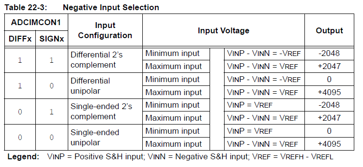
For this example, we're just wanting to stick a potentiometer on AN0, AN1 and AN2 and measure between 3.3V and 0V so I'll be using single-ended inputs only.
/* Configure ADCGIRQENx */
ADCGIRQEN1 = 0; // No interrupts are used
ADCGIRQEN2 = 0;
/* Configure ADCCSSx */
ADCCSS1 = 0; // No scanning is used
ADCCSS2 = 0;
We are not using interrupts and we are not using scanning. That is, we will be manually triggering the ADCs every time we want to read values from them.
/* Configure ADCCMPCONx */
ADCCMPCON1 = 0; // No digital comparators are used. Setting the ADCCMPCONx
ADCCMPCON2 = 0; // register to '0' ensures that the comparator is disabled.
ADCCMPCON3 = 0; // Other registers are “don't care”.
ADCCMPCON4 = 0;
ADCCMPCON5 = 0;
ADCCMPCON6 = 0;
/* Configure ADCFLTRx */
ADCFLTR1 = 0; // No oversampling filters are used.
ADCFLTR2 = 0;
ADCFLTR3 = 0;
ADCFLTR4 = 0;
ADCFLTR5 = 0;
ADCFLTR6 = 0;
We are not wanting any of the fancy digital comparator functionality and we are not wanting to use any of the oversampling filters. Just let us use the ADC already!
/* Set up the trigger sources */
ADCTRGSNSbits.LVL0 = 0; // Edge trigger
ADCTRGSNSbits.LVL1 = 0; // Edge trigger
ADCTRGSNSbits.LVL2 = 0; // Edge trigger
ADCTRG1bits.TRGSRC0 = 1; // Set AN0 to trigger from software.
ADCTRG1bits.TRGSRC1 = 1; // Set AN1 to trigger from software.
ADCTRG1bits.TRGSRC2 = 1; // Set AN2 to trigger from software.
From what I can tell, ADCTRGSNS (ADC Trigger Sensitivity) is set to 0 to trigger on a positive edge (a transition from 0 to 1) or set to 1 to constantly trigger as long as the trigger is set to 1.
For ADCTRG1 through 8 (ADC Trigger) we need to set up how the ADC will be triggered. As we will be triggering it manually from software, we need to set AN0, AN1 and AN2's triggers to 1 to tell the PIC32MZ we will be triggering it from software.
/* Early interrupt */
ADCEIEN1 = 0; // No early interrupt
ADCEIEN2 = 0;
No interrupts. Not today. No.
/* Turn the ADC on */
ADCCON1bits.ON = 1;
/* Wait for voltage reference to be stable */
while(!ADCCON2bits.BGVRRDY); // Wait until the reference voltage is ready
while(ADCCON2bits.REFFLT); // Wait if there is a fault with the reference voltage
Having finally finished the ADC setup, we can turn it on. Once it's on, we need to wait for voltages to stabilise, by checking the BGVRRDY and REFFLT flags) before we can actually enable the inputs and use it.
/* Enable clock to analog circuit */
ADCANCONbits.ANEN0 = 1; // Enable the clock to analog bias
ADCANCONbits.ANEN1 = 1; // Enable the clock to analog bias
ADCANCONbits.ANEN2 = 1; // Enable the clock to analog bias
/* Wait for ADC to be ready */
while(!ADCANCONbits.WKRDY0); // Wait until ADC0 is ready
while(!ADCANCONbits.WKRDY1); // Wait until ADC1 is ready
while(!ADCANCONbits.WKRDY2); // Wait until ADC2 is ready
We are so close now! We enable the clock bias circuitry for each of the ADCs (ANEN0 is ADC0, ANEN1 is ADC1 and ANEN2 is ADC2) and then wait for the ADCs to be ready. And then, finally:
/* Enable the ADC module */
ADCCON3bits.DIGEN0 = 1; // Enable ADC0
ADCCON3bits.DIGEN1 = 1; // Enable ADC1
ADCCON3bits.DIGEN2 = 1; // Enable ADC2
The final step in the setup is to set the Digital Enable DIGEN to 1 . From this point on, ADC0, ADC1 and ADC2 are always sampling from AN0, AN1 and AN2 and are waiting for us to trigger them before they convert the sampled values into the 12-bit format we told them to. This is accomplished by:
/* Trigger a conversion */
ADCCON3bits.GSWTRG = 1;
/* Wait the conversions to complete */
while (ADCDSTAT1bits.ARDY0 == 0);
/* fetch the result */
result[0] = ADCDATA0;
while (ADCDSTAT1bits.ARDY1 == 0);
/* fetch the result */
result[1] = ADCDATA1;
while (ADCDSTAT1bits.ARDY2 == 0);
/* fetch the result */
result[2] = ADCDATA2;
Basically, once you trigger the conversion by setting GSWTRG to 1, ADC0, ADC1 and ADC2 will simultaneously start converting their sampled values to something we can use. Once they're done converting, we can read the values from the appropriate register (ADCDATA0 etc).
I tried the example, it doesn't work, you suck
Indeed. If you try the example as above, it may not work. Why? Because for each of those analog inputs, AN0 to AN2, you have to both set the TRIS value for that port to 1 and set the ANSEL bit for each pin to 1 too. Thankfully, these are the defaults so there's no huge problem there but it is something to be aware of. For reference, this can be done like this:
TRISBbits.TRISB2 = 1; // AN2 = RB2, set it as an input
ANSELBbits.ANSB2 = 1; // Set AN2 to analog mode
My example code, available below, adds the fuses for using FRC at 200Mhz and sets up the wait states and cache. Other than that, it's the same as the example straight from the datasheet.
Categories: pic32