Finishing the USB CDC device
Right. We're finally on the... er... final part of this set of posts on CDC. Woohoo! Today I'll cover my code for handling all the Endpoint 0 transactions and cover how to send and receive data on the bulk endpoints.
Handling the Endpoint 0 transactions for a CDC device
OK. Let's paste this code in:
void USB_EP0_handle_transaction()
{
int cnt;
unsigned char temp_data[7];
USB_LINE_CODING new_line_coding;
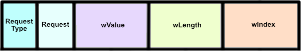
// We're not going to bother with whether bmRequestType is IN or OUT for the most part
switch (USB_transaction.bmRequest)
{
case 0xC:
{
USBE0CSR0bits.STALL = 1;
break;
}
case 0x0:
{
if (USB_transaction.bmRequestType == 0x80) // Get status
USB_queue_EP0(USB_device_description, 0, 0);
if (USB_transaction.bmRequestType == 0x00) // Select function
USB_queue_EP0(USB_device_description, 0, 0);
break;
}
case 0x5: // Set USB address
{
USBE0CSR0bits.RXRDYC = 1;
USB_address = EP[0].rx_buffer[2];
USB_set_address = 1;
break;
}
case 0x6: // Get descriptor
{
switch (USB_transaction.wValue >> 8)
{
case 0x1: // Get device descriptor
{
USB_queue_EP0(USB_device_description, sizeof(USB_device_description), USB_transaction.wLength);
break;
}
case 0x2: // Get configuration descriptor
{
USB_queue_EP0(USB_config_descriptor, sizeof(USB_config_descriptor), USB_transaction.wLength);
break;
}
case 0x3: // Get string descriptors
{
switch (USB_transaction.wValue & 0xFF)
{
case 0x0: // String 0 - Language ID
{
USB_queue_EP0(string0, sizeof(string0), USB_transaction.wLength);
break;
}
case 0x1: // String 1 - Vendor
{
USB_queue_EP0(string1, sizeof(string1), USB_transaction.wLength);
break;
}
case 0x2: // String 2 - Product name
{
USB_queue_EP0(string2, sizeof(string2), USB_transaction.wLength);
break;
}
case 0x3: // String 3 - Serial number
{
USB_queue_EP0(string3, sizeof(string3), USB_transaction.wLength);
break;
}
case 0x4: // String 4 - Configuration
{
USB_queue_EP0(string4, sizeof(string4), USB_transaction.wLength);
break;
}
case 0x5: // String 5 - Interface
{
USB_queue_EP0(string5, sizeof(string5), USB_transaction.wLength);
break;
}
default: break;
}
}
default:
{
break;
}
}
break;
}
case 0x9: // Set interface
{
// Zegads we have enumeration!
break;
}
case 0x20:
{
if (USB_transaction.bmRequestType == 0x21)
{
// Set line coding - host asks us to set our line coding to what it specifies
// Read (wLength) bytes from USB Endpoint 0
USB_receive_EP0(USB_transaction.wLength);
USB_line_coding.baud = ((int)EP[0].rx_buffer[3] << 24) | ((int)EP[0].rx_buffer[2] << 16) | ((int)EP[0].rx_buffer[1] << 8) | EP[0].rx_buffer[0];
USB_line_coding.parity_bits = EP[0].rx_buffer[4];
USB_line_coding.stop_bits = EP[0].rx_buffer[5];
USB_line_coding.data_bits = EP[0].rx_buffer[6];
}
break;
}
case 0x21:
{
// Get line coding - send current line coding to the host
temp_data[0] = USB_line_coding.baud & 0xFF;
temp_data[1] = (USB_line_coding.baud >> 8) & 0xFF;
temp_data[2] = (USB_line_coding.baud >> 16) & 0xFF;
temp_data[3] = USB_line_coding.baud >> 24;
temp_data[4] = USB_line_coding.stop_bits;
temp_data[5] = USB_line_coding.parity_bits;
temp_data[6] = USB_line_coding.data_bits;
USB_queue_EP0(temp_data, sizeof(temp_data), USB_transaction.wLength);
break;
}
case 0x22:
{
if (USB_transaction.bmRequestType == 0x21)
{
// Set line control state
USB_line_control_state = USB_transaction.wValue >> 8;
if (USB_line_control_state != 0)
{
// We're connected now
}
}
break;
}
default:
{
USBE0CSR0bits.STALL = 1;
break;
}
}
}
The comments are fairly self explanatory I think? Nothing fancy there but there are two things I want to mention:
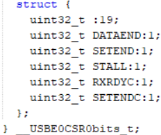
case 0x5: // Set USB address
{
    USBE0CSR0bits.RXRDYC = 1;
    USB_address = EP[0].rx_buffer[2];
    USB_set_address = 1;
    break;
}
As I mentioned a few posts ago, because we are making a device we cannot assign ourselves an address. We have to wait for the host to assign one to us. The value will range from 0 to 127 and will probably differe depending on what USB devices the host already has attached to it. When it sends us an address, we need to put the value into USBCSR0bits.FUNC. I do this in my USB ISR, like this:
if (USB_set_address) // Do we need the set the USB address?
{
    USBCSR0bits.FUNC = USB_address & 0x7F;
    USB_set_address = 0;
}
Secondly, you'll notice this:
USBE0CSR0bits.STALL = 1;
From what I can tell, this will tell the host that the endpoint has stalled either due to an error or because it did not recognise the request. I don't believe this is ever called in my code, I've put it in there because I like to have something in the default case of my switch statements.
OK, so that's all well and good but once your device is enumerated, i.e. recognised and set up by the host, any data it sends will be on the bulk data endpoints. For my code, my bulk data IN endpoint and bulk data OUT endpoint are both endpoint 2. Let's take a look at that in my USB ISR:
if(USBE2CSR1bits.RXPKTRDY)
{
    EP[2].rx_num_bytes = USB_receive_EP2();
    if (USB_RECEIVE_CALLBACK) USB_RECEIVE_CALLBACK(EP[2].rx_buffer, EP[2].rx_num_bytes);
    USBCSR1bits.EP2RXIF = 0;
}
This is slightly different from endpoint 0. This time we don't have RXRDYC we have direct access to RXPKTRDY. More on that later. Let's take a look at the USBreceive_EP2()function:
int USB_receive_EP2()
{
    unsigned char *FIFO_buffer;
    int cnt;
    int bytes_received;

    USBE2CSR0bits.MODE = 0;     // EP2 is RX

    bytes_received = USBE2CSR2bits.RXCNT;

    FIFO_buffer = (unsigned char *)&USBFIFO2;

    for(cnt = 0; cnt < bytes_received; cnt++)
    {
        EP[2].rx_buffer[cnt] = *(FIFO_buffer + (cnt & 3)); // Store the received bytes in array ep0data[].
    }

    USBE2CSR1bits.RXPKTRDY = 0;

    return bytes_received;
}
So the flow here is very similar to endpoint 0 except the one line:
USBE2CSR0bits.MODE = 0; // EP2 is RX
Because I'm using endpoint 2 in a dual role as both a sending and a receiving endpoint, every time I wish to send or receive on it I must set the MODE to the correct value. You can do this just before reading to or writing from the FIFO buffer. 0 means receiving mode and 1 means sending mode.
USBE2CSR1bits.RXPKTRDY = 0;
This is what we were doing indirectly on endpoint 0 by setting RXRDYC to 1, it's just that we now have access to the register directly. We have received the packet, so need to clear the flag.
OK and what's this then?
if (USB_RECEIVE_CALLBACK) USB_RECEIVE_CALLBACK(EP[2].rx_buffer, EP[2].rx_num_bytes);
In my code I've made it possible to have a callback that gets called whenever data is received on endpoint 2. It can be found in the file main.c that comes with the code. In it, I echo back the contents that were received back to the host. I do this by calling USB_send_EP2() so let's have a quick look at that:
void USB_send_EP2(volatile unsigned char *buffer, int size)
{
    int cnt;
    unsigned char *FIFO_buffer;

    USBE2CSR0bits.MODE = 1;     // EP2 is TX

    FIFO_buffer = (unsigned char *)&USBFIFO2;

    for (cnt = 0; cnt < size; cnt++)
    {
        *FIFO_buffer = buffer[cnt]; // Send the bytes
    }

    USBE2CSR0bits.TXPKTRDY = 1;
}
Unlike endpoint 0, we have a maximum packet size of 512 bytes now. As the maximum receive size is also 512 bytes and the PIC32MZ is cutting off packets into 512 byte chunks (thanks to settings in the USBOTG register) I should never receive more than 512 bytes at a time so my code will never end up sending more than 512 bytes at a time. If that were the case, I'd have to handle splitting the data to send up into 512 byte packets, just like I did for the 64 byte long packets on endpoint 0.
Please note that just because you don't receive more than 512 bytes at a time, that doesn't mean the host is limited to 512 characters at once. I pasted the 40,000 characters of one of my random code files into a terminal and my PIC32MZ received it and echoed it back just fine. The host and the PIC32MZ USB peripheral just gave it to me in 512 byte chunks is all.
And with this, the incredibly long series of posts on making a USB CDC device on PIC32MZ are finally done! Next up, an HID device to astound, amaze and annoy!
As always, here's the code!